Lumetra
Lumetra
Lumetra
Engineered for low coplanarity tolerance, automated Pick-and-Place lines, and ruggedized deployments across the Bay Area’s data networking networks.
An in-depth analysis of Signal Integrity, Coplanarity challenges, and B2B deployment frameworks in advanced telecom and enterprise platforms.
The San Francisco Bay Area and Silicon Valley remain the global nucleus of hardware innovation. As hyperscale artificial intelligence (AI) clusters, software-defined networks (SDN), and edge-computing nodes scale exponentially, the requirements for signal pathway physical interfaces have undergone a transformative shift. Historically, standard RJ45 connectors relied heavily on through-hole technology (THT) to provide mechanical strength. However, modern high-density PCB layouts demand space-saving Surface Mount Technology (SMT) and Surface Mount Devices (SMD) to clear paths for high-speed differential signal traces on the inner layers of multilayers PCBs.
For enterprise network switch manufacturers, industrial computer integrators, and optical network providers based in San Francisco, sourcing precision SMT RJ45 female connectors with integrated magnetic components (Magjacks) represents a critical design path. These connectors must withstand rigorous pick-and-place automated optical inspections, high-temperature reflow soldering profiles (often peaking at 260°C for lead-free SAC305 processes), and continuous vibration in high-density rack systems without compromising contact coplanarity or structural integrity.
“In high-frequency networking applications, even a 0.1mm variance in SMT coplanarity can cause dry joints and micro-fractures over repeated mating cycles. Mechanical reliability at the board edge is the silent guardian of cloud uptime.”
On a global scale, the electrical interconnect industry is governed by rigorous mechanical and electromagnetic standards. Organizations like IEEE (through 802.3 Ethernet standards), IEC (via 60603-7 specifications), and ANSI oversee the standardization of modular RJ45 sockets. The integration of magnetic modules directly inside the connector housing (integrated magnetics modules, or IMM) has become the gold standard. These integrated packages act as a low-pass filter, suppressing electromagnetic interference (EMI) and common-mode noise, while providing 1500V AC isolation to protect sensitive PHY chips from electrostatic discharge (ESD) and voltage spikes.
Additionally, the rapid rise of Power over Ethernet (PoE, PoE+, and PoE++ under IEEE 802.3bt) means that modern RJ45 connectors must be capable of carrying up to 90W of electrical power alongside high-speed data transmission up to 10G Base-T. This necessitates high-grade copper alloys (such as Phosphor Bronze) with thick Gold plating (up to 50 micro-inches) at contact points to prevent contact erosion due to electrical arcing when plugs are disconnected under load.
For hardware procurement teams based in the San Francisco Bay Area, balancing prototype agility with high-volume cost containment is a critical operational dynamic. This is where the structural advantages of established Chinese electronics manufacturing hubs come into play. By operating specialized production centers equipped with fully automated high-speed stamping presses, advanced plastic injection molding systems, and automated winding arrays for the inner magnetic inductors, Chinese factories offer an unbeatable ratio of quality, speed, and unit economy.
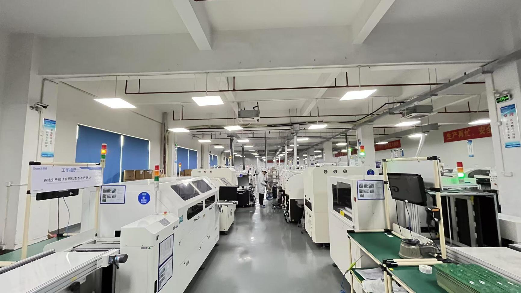
The manufacturing ecosystem in China allows factories to integrate raw material procurement, PCB assembly, automated winding, terminal insertion, and final functional testing into a centralized flow. This localized industrial concentration reduces the lead times for custom-tooled RJ45 connectors down to 3–4 weeks, compared to 8–12 weeks in European or North American facilities. High-density packaging solutions, such as automated Tape and Reel (T&R) carrier tape, are standard, allowing US-based contract manufacturers (EMS) to directly load components onto automated high-speed surface-mount assembly lines without manual sorting.
San Francisco’s dynamic commercial landscape features several distinct environments where SMT RJ45 female connectors serve as structural links:
High-Density AI & Machine Learning Compute Arrays: In South of Market (SoM) and Mission Bay labs, hardware startups develop accelerator cards requiring RJ45 modular jacks for out-of-band management systems (IPMI). The low-profile surface mount footprint allows these connectors to sit underneath massive heat sinks on tightly packed server motherboards.
Industrial IoT & Smart Infrastructure: The Port of San Francisco and smart city utilities deploy municipal gateway nodes. SMT RJ45 connectors equipped with robust shielding boots are selected here to resist harsh physical environments, high humidity, and salt spray while maintaining data transmission.
Edge Devices & Biomedical Instrumentation: Tech parks in South San Francisco house medical technology manufacturers whose surgical devices and imaging panels require precise PCB integration, where any connection failure might disrupt critical data streams.
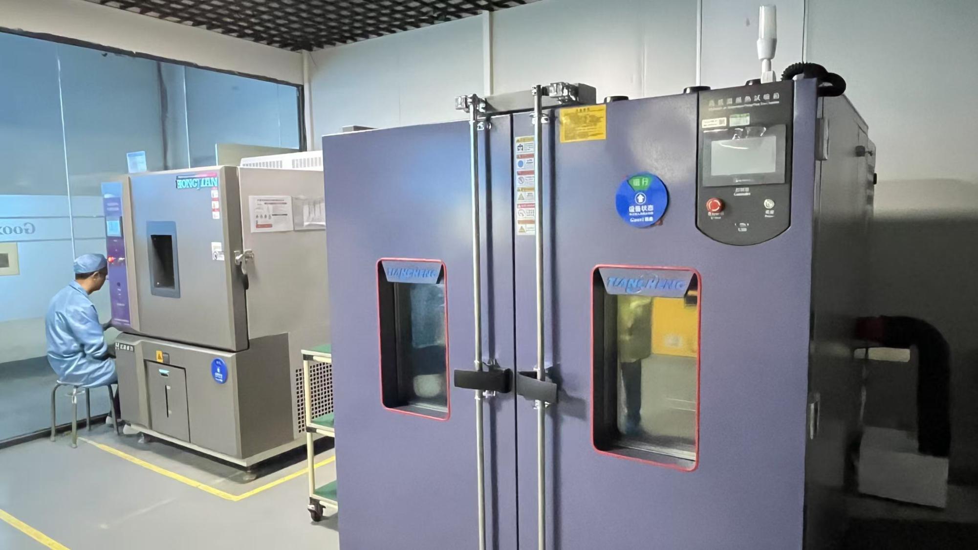
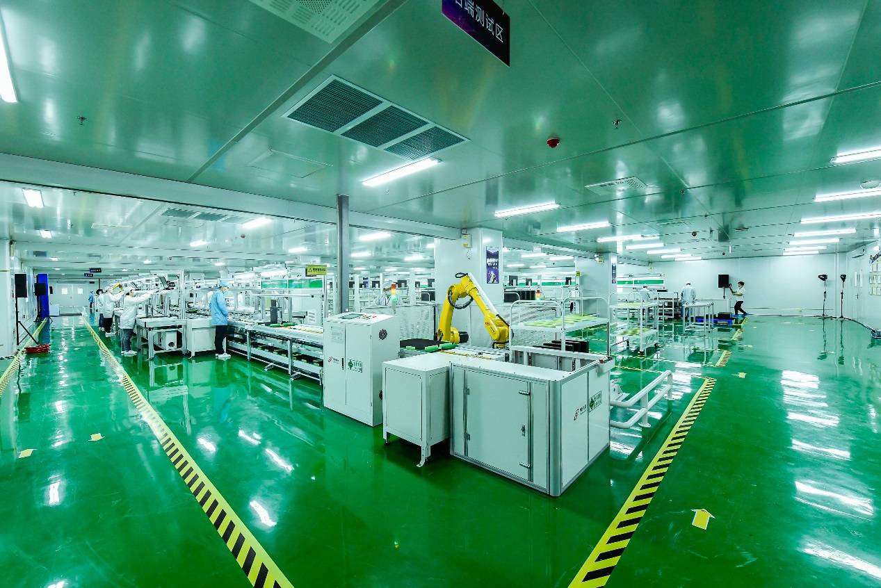
Behind our export capabilities lies a highly automated facility designed for optical components and precision magnetic-integrated interconnect solutions.
Lumetra Optoelectronics Technologies Co., Ltd. is a professional manufacturer specializing in high-speed optical transceivers and fiber optic communication solutions for datacom, telecom, and cloud infrastructure applications. Founded in 2016, the company has developed into a reliable supplier with strong engineering capabilities and global export experience.
Operating from an 8,500㎡ production facility, our operations support highly controlled assembly and testing methodologies. Backed by 11 years of overall industry expertise and 7 years of active international business channels, our annual export revenue reaches approximately USD 18 million.
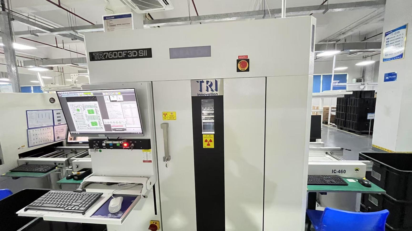
We maintain strict quality control standards, leveraging automated optical testing, environmental stress screening, and manual inspection. Our dedicated quality assurance team consists of 48 trained inspectors ensuring that every batch of SMT RJ45 connectors and optical transceivers aligns with international norms.
With a diversified trade background across OEM and ODM markets, Lumetra serves clients in North America, Europe, Southeast Asia, and the Middle East. We maintain active partnerships with over 1,200 supply chain providers to secure reliable raw materials and mechanical parts. Our R&D team of 86 engineers focuses on signal integrity, thermal management, and custom protocol configurations.
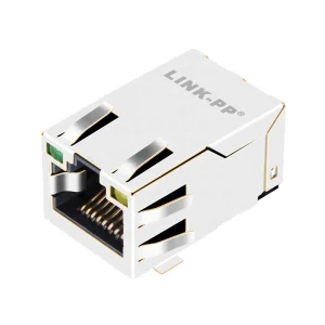
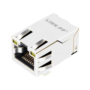
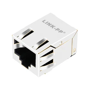
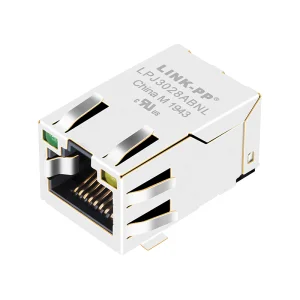
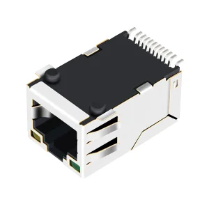
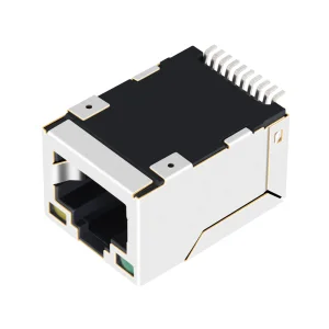
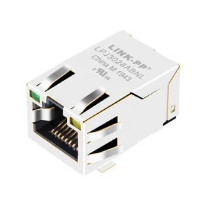
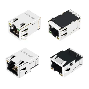
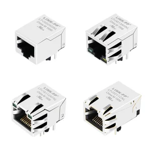
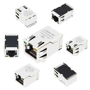
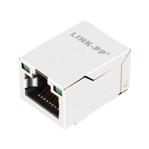
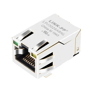
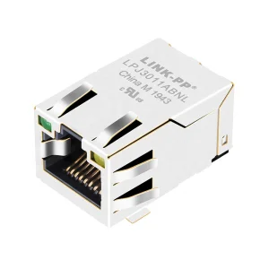
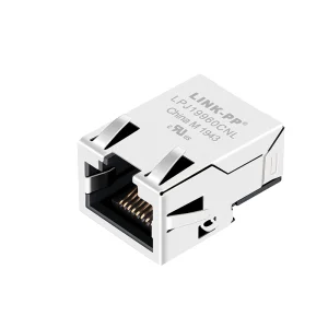
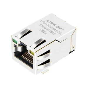
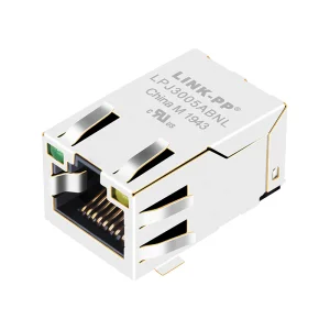
A comprehensive inventory of modular sockets, featuring shielded structures, integrated LEDs, and varied pin configurations to match diverse routing demands.
Understanding critical engineering and trade parameters prior to placing high-volume production orders.
For automated surface-mount assembly, the standard coplanarity tolerance limit for RJ45 leads is 0.1mm (0.004 inches). Any value exceeding this limit risk causing open contacts or weakened joints during the reflow phase. We run inline automated optical measurement (AOI) scanner passes on 100% of our products to check each lead profile prior to packaging.
Integrating the isolation transformer, common-mode chokes, and resistors inside the metal shield of the connector saves up to 50% of the board space required by discrete layouts. It also positions the noise-filtering elements closer to the physical interface, which cuts down EMI radiating onto neighboring differential tracks.
We use Liquid Crystal Polymer (LCP) and High-Temperature Polyamide (PA9T) for our SMT connector bodies. These plastics feature a heat distortion temperature exceeding 280°C, enabling them to survive peak lead-free reflow runs of 260°C without bubbling, deformation, or contact terminal shifting.
Yes. Supported by our R&D group of 86 engineers, we can customize shielding structures, grounding configurations, pin layouts, and integrated LED configurations (including yellow/green dual combinations). Custom engineering requests can also encompass specific compatibility options for targeted PHY chips.
Standard tooling designs ship within 2 to 3 weeks, while custom injection molding configurations can take between 4 to 6 weeks. Our international logistics network supports direct air cargo deliveries to San Francisco International Airport (SFO) or ocean freight shipments handled through the Port of Oakland.
Get in touch with our team today to request complete component datasheets, 3D step files, layout recommendations, and rapid B2B pricing quotes.
Send Inquiry Now